Back-end Design

VLSI Physical Design (PD)

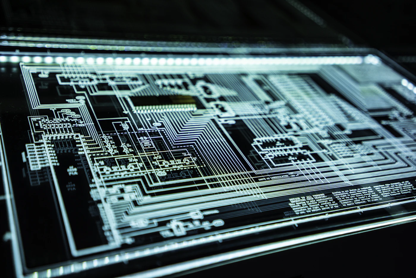
Comprehensive ASIC Physical Design training: Netlist → GDSII with tools, projects, and interview preparation.

Hybrid Intermediate 4 – 6 Months (Industry-Oriented Training Program)
Overview
The VLSI Physical Design (PD) Training Program is designed to provide comprehensive knowledge of the complete ASIC implementation flow used in the semiconductor industry. The course combines fundamental theory, practical tool-based training, and real-time design projects to prepare candidates for careers in VLSI design and chip implementation.
Key features
This page focuses on highlights and outcomes (no price shown).
Back-end Design
Industry-oriented Physical Design flow Hands-on, tool-based practical training Complete Netlist → GDSII flow coverage Real-time industry project work Interview preparation + mock interviews
Syllabus
Modules are editable in Admin.

  • The VLSI Physical Design (PD) Training Program is designed to provide comprehensive knowledge of the complete ASIC implementation flow used in the semiconductor industry.
  • The course combines fundamental theory, practical tool-based training, and real-time design projects to prepare candidates for careers in VLSI design and chip implementation.

  • Digital Circuit Fundamentals – Basic logic gates, combinational and sequential circuits
  • CMOS Technology & Layout Principles – CMOS devices, design rules, and layout basics
  • Linux Operating Environment – Commands, file management, and scripting basics
  • ASIC / SoC Design Methodology – Overview of semiconductor design lifecycle
  • PDK & Technology Libraries – Understanding process technologies and libraries
  • Standard Cells & Macro Libraries – Cell structures and library usage
  • Timing Constraints & SDC – Defining timing requirements for designs
  • Static Timing Analysis (STA) – Timing verification and analysis fundamentals

  • RTL Synthesis Flow – Converting RTL code into gate-level netlist
  • Pre-Layout Timing Analysis – Early timing validation before implementation
  • Design for Testability (DFT) – Introduction to scan structures and test concepts
  • Physical Design Flow Overview – Steps involved in ASIC physical implementation
  • Floorplanning & Design Planning – Core area definition and macro placement
  • Power Planning & Routing – Power grid structure and connectivity
  • Pre-Placement & Physical Cell Preparation – Preparing the design database
  • Standard Cell Placement Techniques – Automatic and optimized placement
  • Scan Chain Optimization – Reordering scan chains for improved routing
  • Pre-CTS Timing Optimization – Timing fixes before clock implementation
  • Clock Tree Synthesis (CTS) – Building balanced clock distribution networks
  • Post-CTS Timing Optimization – Timing adjustments after CTS
  • Routing & Signal Connectivity – Global and detailed routing techniques

  • Physical Verification Flow – DRC, LVS and layout verification concepts
  • RC Extraction – Extraction of parasitic resistances and capacitances
  • Sign-Off Timing Analysis – Final timing validation using STA
  • Timing Closure Techniques – Resolving setup and hold violations
  • Engineering Change Orders (ECO) – Late-stage design modifications
  • Logical Equivalence Checking (LEC) – Functional verification after changes
  • IR-Drop & Electromigration Analysis – Power integrity and reliability checks

  • Low Power Design Techniques & UPF
  • TCL Scripting for Design Automation
  • Advanced Static Timing Analysis Concepts
  • FinFET Technology & Double Patterning Basics
  • Physical Design Challenges in 16nm & 7nm Technology Nodes
  • Make Flow & LSF Job Scheduling

  • Complete Physical Design Flow Implementation
  • Multi-block design projects
  • Real-time design scenarios and debugging

  • Professional Soft Skills Development
  • Technical Presentation Practice
  • Resume Preparation & Profile Building
  • Interview Preparation Sessions
  • Mock Technical Interviews with Experts

  • Synopsys ICC2
  • Cadence Innovus
  • PrimeTime (PT)
  • Tempus STA
  • Linux Environment
Outcomes
Understand the complete ASIC implementation (Netlist → GDSII) flow
Perform floorplanning, placement, CTS and routing with practical understanding
Develop STA and timing closure skills (setup/hold) with real reports
Gain sign-off awareness: DRC/LVS, IR-drop and electromigration concepts
Build interview readiness through projects, presentations and mock interviews
Course Duration
Featured
4 – 6 Months
Industry-Oriented Training Program
Tool-based, hands-on training
Real-time projects and debugging
Daily doubt support
Mock interviews + placement support
Complete PD flow: Floorplan → Place → CTS → Route
STA + timing closure mindset
Sign-off basics: DRC/LVS, IR/EM
Get schedule & batch details
Request details
Quick response
Share your details—our team will suggest the right plan and next steps.

Request details